6/24/2024 8:45 PM: -- Breadboard CoCo - Part 3: The Schematics

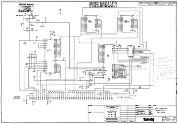
I have found 4 schematics.
Pretty sure all these are almost identical. At least 3 of them. The other seems to be for the 64k model and the rest is near identical.
If you check out the SAM reference and other locations you begin to realize that the block diagram of the main chips (aka the "reference schematic") is precisely what Radio Shack took and added the CoCo's I/O to it. The way that the core chips were interconnected was already pretty much laid for them.
The 16 bit address bus is directly connected to the CPU, the SAM, the ROMS, and the cartridge slot.
The data bus is directly attached to the CPU, the RAMS, the 74LS244, the ROMS, the PIA's, and the cartridge slot.
The 74LS244 (tri-state line driver) allows switching the data out pin of the 8 RAMS to go between the 8 bit CPU data lines (D7-D0) to the 8 bit data inputs of the 74LS273 (flip/flop register) which in turn clock the data into the the VDG to feed it video RAM.
The /MRD coming from the 74LS138 is used to switch the 74LS273. This signal is generated from the SAM and then demultiplexed by the 74LS138.
The /RAS signal from the SAM is used as the clock for the 74LS273.
The 74LS02 turns off ROM under certain conditions which are not clear to me yet. But we will be looking at it in detail.
To breadboard a CoCo1 then we need to connect the pins of these main chips together. This will require some planing and next I'll create a new schematic in KiCAD with these connections. And make a "net list" that I can follow when connecting these up on the breadboard.
Once we have enough of the circuits put together we will study the signals more in depth.